A brief History
I will tell you some history now. Intel (Integrated Electronics) developed its first microprocessor chip 4004 in 1971 which was 4 bit. Intel opened the 8 bit market in 1974 when they released 8008 and 8080. During that time Motorola released its first one, 6800 which was also 8 bit.
I will tell you some history now. Intel (Integrated Electronics) developed its first microprocessor chip 4004 in 1971 which was 4 bit. Intel opened the 8 bit market in 1974 when they released 8008 and 8080. During that time Motorola released its first one, 6800 which was also 8 bit.
 Intel Corporation introduced 8051 series MCU in 1981. It was built according to the Harvard Architecture. It is referred to as the MCS-51 series. Many different vendors use this MCS-51 architecture originally developed by Intel.
Atmel Corporation introduced its first 8 bit Flash based microcontroller in 1994 which was a MCS-51 derivative. In 1996 Atmel released 8 bit AVR RISC microcontroller for the first time. Two students at the Norwegian Institute of Technology (NTH), Alf-Egil Bogen and Vegard Wollan conceived AVR which follows the Modified Harvard Architecture.
What does the term AVR stands for is not mentioned clearly. Many people think AVR stands for Alf Vegard RISC. From now on we will use the term AVR to refer to Atmel’s 8 bit AVR microcontrollers.
Microchip Technology has a popular series of uCs called PIC. If you want to know more about PICs, you can visit the Microchip Website.
The Architecture of AVR
The term RISC stands for Reduced Instruction Set Computing. The RISC processors are designed to run faster and provide better performance by using a reduced number of instructions.
If you are interested to read more about RISC you can visit this Wiki Link.
If you are interested to read more about RISC you can visit this Wiki Link.
The Von Neumann Architecture uses the same memory space for instructions and data. It uses the same bus to access them. The Harvard Architecture uses separate memory space for storing instructions and data. It uses separate buses for accessing them. If you want to know more about Harvard Architecture you can visit this Wiki Link.
The processors which use the Von Neumann Architecture can’t access the instructions and the data at the same time while the one’s using the Harvard Architecture can access them simultaneously.
What does the term '8-bit' mean?
The MCUs we are going to use are 8 bit. It means that they can process 8 bits of data at a time. 8 bits equal to 1 byte. It executes 1 byte data every cycle. If any instruction or data is larger than 8 bits, then the uC breaks it into 8 bit parts and executes them one by one. The meaning of 8 bit does not end here.
Most of the registers are of 8 bits in size. That means a register can hold a maximum value of 11111111 in binary or 255 in decimal. Sometimes the microcontroller combines two 8 bit registers to represent one 16 bit register which can hold larger values.
The microcontroller has input/output (I/O) ports. Each port has 8 pins.
I hope you get the idea of 8 bit uC. There are 16 bit and 32 bit microcontrollers too. We can use them for designing large and fast systems. At present our computers use 64 bit processors.
Which uC to use?
The selection depends on our application. There are different models of AVRs available to serve our needs. You can visit this page of Atmel to know more, Atmel AVR.
In our country 8 bit mega AVRs are available. This page lists all the models of the mega series AVRs produced by Atmel, ATmega List.
We are going to use ATmega8 in the tutorial projects. You will get it in the electronics market. I will try to provide a buyer’s guide soon to help you out on the devices you need to collect.
The ATmega8
The name tells us one of the most important info. ATmega8 means Atmel’s Mega Series AVR with a flash memory of 8 kilobytes. ATmega16 & ATmega32 have 16 and 32 kilobytes of flash memory respectively.
 |
| Figure: The one I bought last week, ATmega8L. |
After you have downloaded the PDF, take a look. The first page lists all the features in a nutshell. Read it carefully. You might find many terms unfamiliar. Don’t worry; we will learn those step by step.
From the list of features, try to figure out the following,
What are the available packages and what is the amount of pins?
How many I/O lines or Ports?
What is the CPU architecture?
What is the clock speed supported by the CPU?
Is there any built in oscillator?
What is the amount of program memory?
Does the chip include EEPROM? If so, how much does it carry?
What is the amount of RAM?
Does the uC have Timer? If it has then how many?
Is there any support for Pulse Width Modulation (PWM)?
Does the uC chip include Analog to Digital Converter (ADC)?
Does the uC support serial communication (USART)?
Does the uC support Interrupts?
What is the Power Consumption?
What is the operating voltage?
Let’s talk about the important features.
Package and Pin Configuration
The ATmega8 is available in PDIP, MLF and TQFP packages. We will use PDIP (Plastic Dual-in-Line) package. This package has 28 pins. The pin configuration is given below,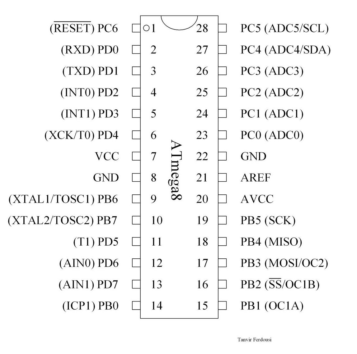 |
| Figure: ATmega8 Pin Diagram |
Input/Output (I/O)
There are 3 bidirectional ports in the ATmega8. A Port is simply a bundle of pins. As it is an 8 bit uC, each port has 8 pins. Only Exception is that Port C has 7 pins. Port B consists of 8 pins starting from PB0 to PB7. Similarly,
Port C: PC0 to PC6 (7pins)
Port D: PD0 to PD7 (8pins)
Remaining Pins
There are 5 more pins. They are described below,
PIN Number
|
Name
|
Purpose
|
7
|
VCC
|
Main Power Supply (Digital)
|
8
|
GND
|
Ground
|
20
|
AVCC
|
Power Supply for ADC*
|
21
|
AREF
|
Analog Reference pin for ADC
|
22
|
GND
|
Ground
|
ADC is a component which is built in the uC chip. We will use pin 7 and pin 8 to connect power supply +5V and Ground respectively to power up our microcontroller.
The bracketed terns indicate the secondary functions the pins can perform. We will encounter them when needed.
The bracketed terns indicate the secondary functions the pins can perform. We will encounter them when needed.
Power Requirements
Locate these lines in the first page of the datasheet,
Operating Voltages
– 2.7 - 5.5V (ATmega8L)
– 4.5 - 5.5V (ATmega8)
There are two variants of ATmega8, these are ATmega8 and ATmega8L. This is the specified voltage range for the two variants. ATmega8L has wider range, it supports both 5V and 3.33V logic. We will implement 5V logic in our circuits.
I hope you found the following lines,
Power Consumption at 4 Mhz, 3V, 25°C
– Active: 3.6 mA
– Idle Mode: 1.0 mA
– Power-down Mode: 0.5 μA
CPU & Clock
The CPU is the core of the MCU. It executes instructions one by one. The CPU is driven by a clock source. A clock source is the heart of the microcontroller. It supplies the clock signal.
In digital logic you will commonly hear the term clock. A clock signal is needed to run the counters and the registers. Each clock pulse makes the counter count. The registers also manipulate data with the help of clock pulses.
A clock provides pulses at regular intervals. In other words, a clock signal has a certain frequency. It controls the speed of the CPU operation. At each clock pulse, the CPU executes one 8 bit instruction. The frequency of the clock signal is the frequency of the CPU operation. I hope you found the following data,
–Up to 16 MIPS Throughput at 16 MHz
Speed Grades
– 0 - 8 MHz (ATmega8L)
– 0 - 16 MHz (ATmega8)
The first line says that the CPU can execute up to 1 Million Instructions per Second (MIPS) if it operates at 16 MHz. In other words, it can execute 1 instruction at each clock cycle.
The MCUs can operate at any frequency between the given speed range. The maximum frequency supported by ATmega8 is 16MHz and ATmega8L is 8MHz.
One might wonder, is the frequency fixed or variable? In fact, we can choose the frequency and adjust a clock source accordingly. An oscillator acts as the clock source. For example, if we want to run the CPU at 4 MHz, we will adjust our oscillator to provide a 4 MHz clock signal. The CPU will constantly operate at 4MHz.
Clock Source
In the earlier days an external oscillator was needed to provide the clock signal to the CPU. The AVR microcontrollers have internal RC oscillator which makes our job easier. Notice the line,
– Internal Calibrated RC Oscillator
ATmega8 has an internal calibrated RC oscillator which is by default set to 1 MHz. We can configure it to operate at 2, 4 and 8 MHz too.
However, if required, you can connect an external oscillator. The ATmega8 has two pins marked XTAL1 and XTAL2 for connecting external oscillators.
Is the Internal RC oscillator sufficient?
For our most of our tasks it will be sufficient. There are some limitations of RC oscillators. The frequency of the RC oscillator is not purely constant. It can vary with voltage, temperature etc. The tolerance is quite high, around 3%. That means if we set it to 1 MHz, it can operate at any value between 0.97 MHz to 1.03 MHz. It is not suitable for applications where precise measurement of time is required.
 |
| FIgure: Crystal Oscillator connection (optional) as given in the datasheet. |
If we build a system where timer accuracy is a concern, we can use an external crystal oscillator and connect it to the XTAL pins as shown. Crystal oscillators are much more accurate.
We can happily stick to the internal oscillator for normal operations. It is chosen as the clock source and is set to 1 MHz by default. For now, we do not need to worry about oscillators.
Memory
Notice these lines,
– 8K Bytes of In-System Self-programmable Flash program memory
– 512 Bytes EEPROM
– 1K Byte Internal SRAM
We will store our program in the flash memory. It is non volatile and permanent. We can program the AVR while it is operating in the system. We can write and rewrite our program many times.
EEPROM stands for Electronically Erasable Programmable Read Only Memory. We can use it to store data. It is non-volatile so it will retain the data. There are 512 bytes of EEPROM.
There is 1 kilobyte of Static RAM in ATmega8. Static RAM is a kind of fast access RAM used by microcontrollers; remember our computers use DRAM (Dynamic RAM).
Timers

The AVRs have built in timers to count time. A timer is a combination of some hardware and a few dedicated registers to facilitate the counting of numerical values. Look at these lines,
– Two 8-bit Timer/Counters with Separate Prescaler, one Compare Mode
– One 16-bit Timer/Counter with Separate Prescaler, Compare Mode, and Capture Mode
As you can see, there are three timers in total. Two 8 bit timers and a 16 bit timer are given in the package. An 8 bit timer can count up to a maximum value of 11111111 in binary or 255 (decimal) in its count register after which it overflows. A 16 bit timer can count up to a maximum value of 1111111111111111 (binary) or 65,535 (decimal) in its count register after which overflow occurs.
The timers can be driven by either the internal clock which drives the CPU or by an external clock if we want.
Prescaler: A Prescaler divides the clock frequency if required. For example, if we want to count at 4 MHz but we have a clock frequency of 16 MHz, then we will divide the frequency by 4 using the prescaler.
The timer modes will be discussed later in the Timer Chapter.
Pulse Width Modulation (PWM)
This is a very useful and important feature. The timers have PWM modes. We use these to generate PWM signals. Somw of us may not be familiar with the term PWM. PWM is a technique of controlling power flow in electrical devices. See this line in the datasheet,
– Three PWM Channels
PWM has many applications. Starting from the speed control of motors up to brightness control of your LCD screen you are looking at are done using PWM. The Switch Mode Power Supplies use PWM. PWM signals drive power electronic devices.
Analog to Digital Converter (ADC)
This will be very useful in signal processing applications.
Analog to Digital Converter (ADC)
 | |
| Figure: An ADC converts analog signals to digital signals |
This is another important feature. There will be many occasions where we will need to convert an analog signal to digital signal. The uC deals with digital signals only. So if we want to process analog signals, first we have to convert it into a digital signal and then feed it to the uC.
Fortunately our uC includes ADC in it. We can connect analog sources directly to the uC pins. We don't need any separate ADC to do this conversion.
Fortunately our uC includes ADC in it. We can connect analog sources directly to the uC pins. We don't need any separate ADC to do this conversion.
– 8-channel ADC in TQFP and QFN/MLF package
Eight Channels 10-bit Accuracy
– 6-channel ADC in PDIP package
Six Channels 10-bit Accuracy
Interrupts
This is one of the most useful features in many uC based systems. We know from chapter 2 that the uC follows the main routine written in the main() function where it circulates in an infinite loop.
If we want our microcontroller to respond to special situations and conditions, we use the interrupt feature. For interrupts we can write additional routines which are called Interrupt Sub-Routines (ISR) outside the main function as ISR().
I described an Automated Water Pump Control system in the last chapter. We want to install a switch such that if the switch is pressed, the system makes the motor an emergency stop and does not start it again until we press another button.
In this case the uC has to come out of its main routine and follow a subroutine which we will describe in the ISR()code block. The subroutine instructs the uC to stop the motor immediately. This is how interrupt works. It interrupts the main routine.
A uC does not know when an interrupt will occur but it knows what to do if any certain interrupt occurs. We have to describe the task which we want our MCU to perform in the ISR block of that certain interrupt.
The Interrupt feature requires detailed explanation, I will try it later. You will find this line in the datasheet,
– External and Internal Interrupt Sources
Interrupt sources can be either internal or external. The emergency stop switch in the pump example is an external interrupt source.
No comments:
Post a Comment